Interface
1. Interface Design Diagram
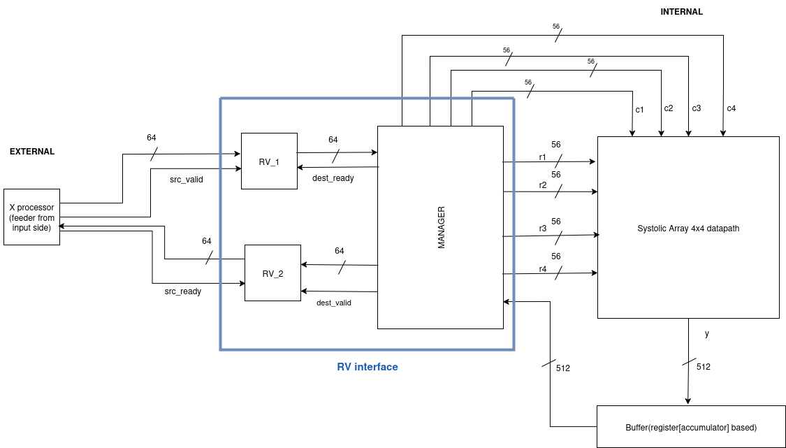
Main Parts of Interface:
1. Ready-Valid Protocol
2. Input Manager
3. Output Manager
EXPLANATION
1. READY-VALID PROTOCOL
PinOut
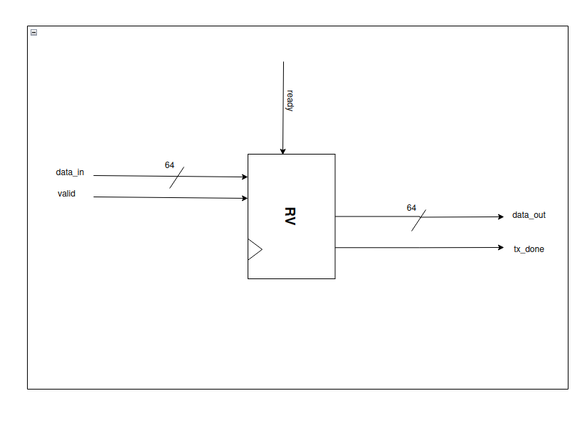
Inputs:
- ready – Indicates that the receiver is ready to accept data.
- valid – Indicates that the sender has valid data.
- data_in – 64-bit input data.
Outputs:
- data_out – 64-bit output data.
- tx_done – Goes high whenever data_out is successfully transmitted.
Design Diagram
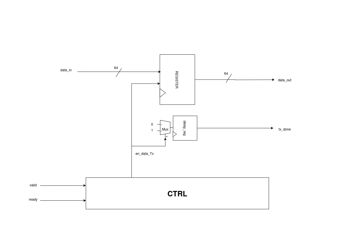
Explanation
- Whenever valid becomes high,
data_inis received. - When both valid and ready are high:
en_data_Txgoes high → handshaking occurs.data_outis produced in the next cycle (64 bits).tx_donesignal goes high whenever the respectivedata_outis available.
How does tx_done work?
en_data_Txgoes high when handshaking occurs.- A multiplexer (MUX) uses
en_data_Txas the select signal. - When
en_data_Tx = 1, the MUX outputs 1. - This output passes through a delay register, producing
tx_donein the next clock cycle.
Why use a delay register?
- Without the delay register,
tx_donewould assert one cycle earlier than the availability ofdata_out. - The delay register ensures
tx_donealigns with the exact cycle whendata_outis valid, confirming the output data is ready.
State Transition Graph (STG)
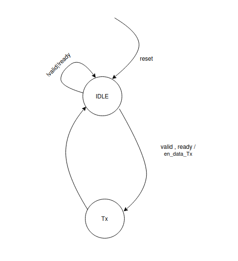
Explanation
I. IDLE
- On reset, the system enters the IDLE state.
- If either
validorreadyis low, the system remains in IDLE. - When both
validandreadyare high, handshaking occurs, and the system transitions to the Tx state.
II. Tx
- In this state,
validandreadybeing high indicate that handshaking has occurred. - The
en_data_Txsignal is asserted (goes high), initiating the data transfer. - Immediately after this, the system returns to the IDLE state.
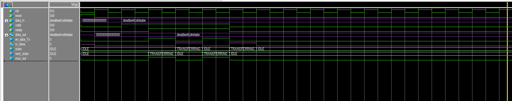
Simulations:
2. INPUT MANAGER
PinOut
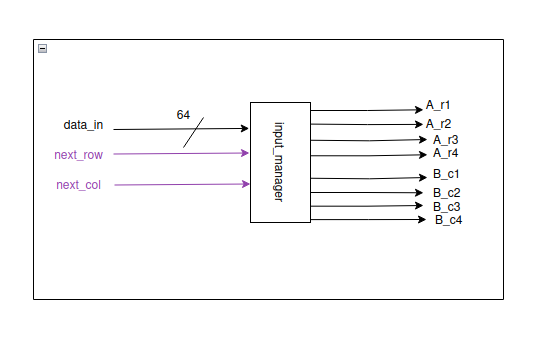
Inputs:
- data_in – 64-bit input data.
- next_row – Signal to indicate the next row of the matrix.
- next_col – Signal to indicate the next column of the matrix.
Outputs:
- A_r1, A_r2, A_r3, A_r4 – 56-bit outputs for rows 1 to 4.
- B_c1, B_c2, B_c3, B_c4 – 56-bit outputs for columns 1 to 4.
- Each row/column has 7 elements, and each element is 8 bits → 7 × 8 = 56 bits.
Working:
- The Input Manager is combined with the input datapath, which is explained in the following section.
3. OUTPUT MANAGER
PinOut
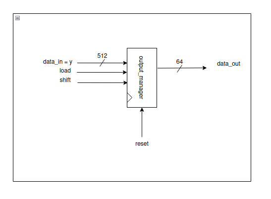
Inputs:
- load – Signal to load the input data.
- shift – Signal to shift the data.
- reset – Resets the internal state of the output manager.
- data_in – 512-bit input data (y from processing elements).
Outputs:
- data_out – 64-bit output data, produced eight times from the 512-bit input.
Design Diagram
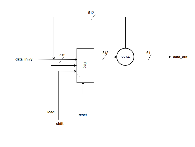
Explanation
- The Systolic Array produces 512 bits output (16 PEs × 32 bits each).
- These 512 bits serve as
data_in/yfor the Output Manager. - The Output Manager acts like a data feeder, mainly implemented as a shift register.
- The first 64 bits are taken from the MSB side when
loadis high. - For the remaining seven 64-bit chunks:
- Wait for the
shiftsignal. - Each time
shiftgoes high, the next 64-bit chunk is produced asdata_out. - In this way, the eight 64-bit outputs are obtained sequentially.